Making the PCB
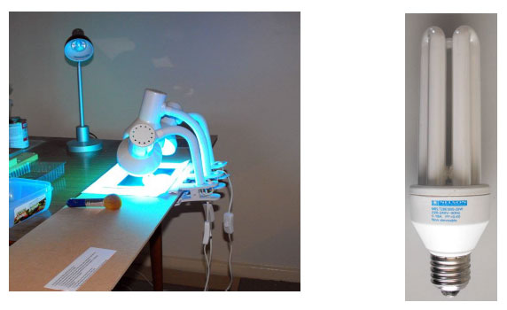
The board was exposed on the kitchen table using three bed-side lamps fitted with “insect” blue lights. The lights are marked MELT28ESBS-28W by Nelson. And yes it is an Edison style fitting.
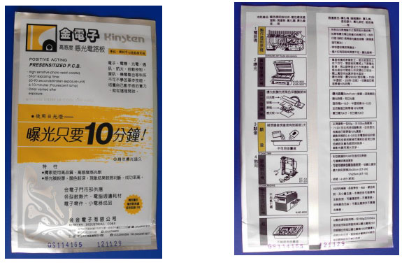
The PCB was made using a Kinsten single-sided positive resist board measuring 165 mm by 114 mm. The board has a thickness of 1.6mm and a copper density of 1 ounce per square foot.
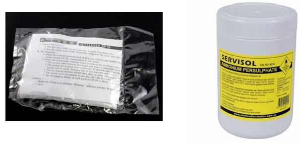
After exposure to the UV lamps for 5 minutes, the board was developed using Kinsten DP-50 (sodium metasilicate) and then etched using Ammonium Persulphate.
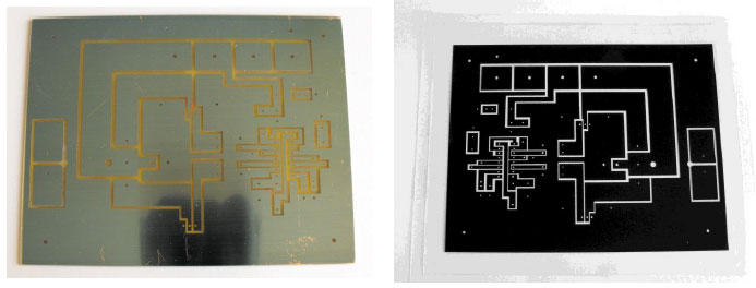
On the left is the board after development and etching, and on the right the PCB template. The side of the template shown is that side placed on the photo resist side of the board. Only those areas exposed to UV light are removed with the DP-50 developer. Hence the term positive resist.
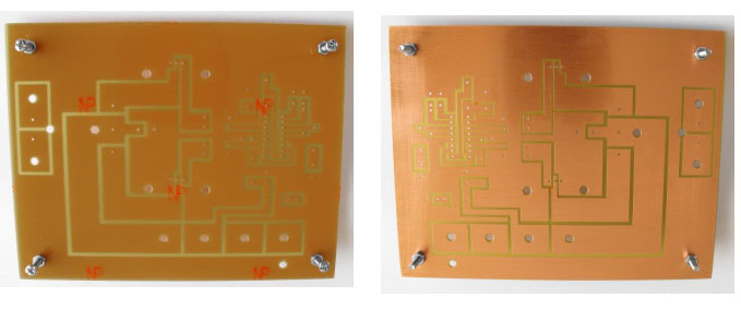
After drilling, the board was coated with two layers of acrylic to protect the surface and stop the copper from oxidizing. The screws in the photos are used to support the board during the coating process. The photo on the left shows the component side of the PCB. The photo on the right shows the copper side.
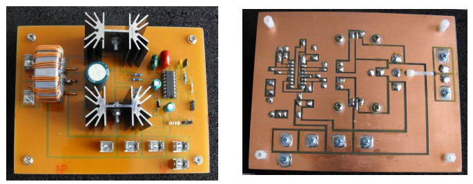
The above photo shows the completed circuit board with components. It is not a crowded board and this is my preference. The heatsinks are attached to the board with screws. The switch, power supply input, amp meter and fuse use spade connectors for easy and quick access. The male PCB spade connectors were screwed to the appropriate PCB pad after a 1 mm thick layer of solder had been laid down. Each screw has a flat washer above a star washer to provide a secure attachment to the soldered pad. The same method was used for the output inductor connections. The output inductor is secured to the board with a cable tie and rests on a 1mm thick silicone support. The board rests on 10mm high threaded Teflon stand-offs as shown in the photo on the left.
A FEW NOTES ON PCB TRACK WIDTH
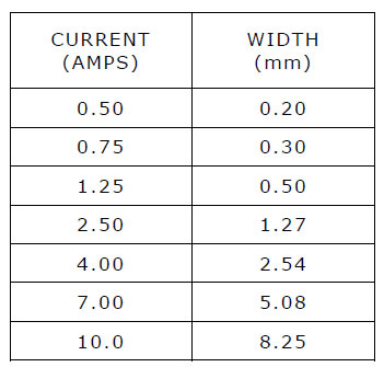
When designing a PCB you must also consider the amount of current that a circuit will handle, continuously and also the likelihood of peak surges. It is difficult to give an exact formula and though online calculators are available many considerations must be taken into account. Will the circuit be open to air or encapsulated in epoxy or some other potting resin. What is the density of the copper laminate - 1 or 2 ounces per square foot, and so on? The following table gives minimum track widths for a 1.6mm (0.063") thick, 1 ounce per square foot copper FR-4 fiber glass laminate board to supply adequate current to components in a non-encapsulated circuit without significant temperature rise. For a 100C temperature rise, minimum track widths are.
I always estimate maximum current consumption, and then multiply track width by at least 2. Of course I have no production or commercial considerations – the attraction of being a self-reliant hobbyist who focuses on one-of-a-kind creations.