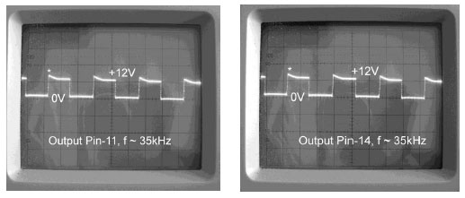
Shown above are the output waveforms of Pin-11 and Pin-14 of the SG3525 PWM chip. They look identical until compared with the dual channel function of the scope. The tip of the peak marked with a “*” is an artifact arising from leakage inductance and the gate capacitance of the IRF540N. See below.
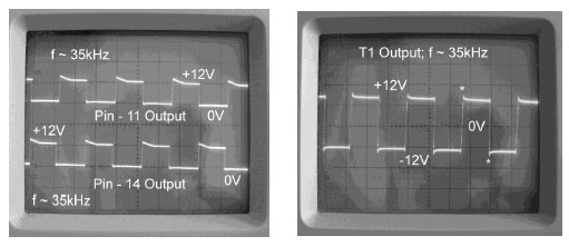
The trace on the left shows the phase characteristics of the SG3525 PWM chip outputs for driving the gates of the IRF540N Mosfets. The trace on the right shows the output from T1, the toroidal inductor. T1 “effectively” flips one of the waveforms – in simple terms of course.
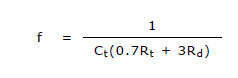
A BRIEF NOTE ON THE SG3525AN
The best source of information on this device is the data sheet and the relevant application notes, but a few quick comments might be useful. Below is a diagram of the pin layout as used in the project.
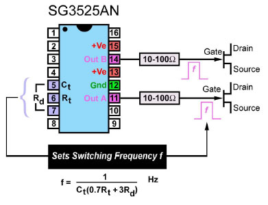
Of particular importance to the existing design are Pins 5, 6, 7, 11 and 14. Pin 11 and Pin 14 are the gate drive output pins and these provide the switching pulses to drive the gates of the MOSFETs via a suitable resistor. The output frequency of Pin 11 and Pin 14 is set by the timing capacitor Ct connected to Pin 5, and the timing resistor Rt connected to Pin 6. A small value resistor between Pin 5 and Pin 7 sets the “dead-time” of the output (see data sheet). The frequency output from Pin 11 and Pin 14 is then given by the formula:
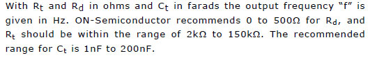
A BRIEF NOTE ON THE IRF540N MOSFET
The best source of information on this device is the data sheet and the relevant application notes, but a few quick comments might be useful. Below is a diagram of the pin layout for this device.
MOSFETs can be damaged by static charge when handling, testing or installing into a circuit. So treat them with care. Observe good ESD practices.
Beware of unexpected gate-to-source voltage spikes. Excessive voltage will punch a hole through the gate-source oxide layer. This will destroy the device – permanently. Remember transient gate-to-source over-voltages can be generated that are unrelated to the amplitude of the applied drive signal.
Beware of Drain voltage spikes induced by switching. Self-inflicted overvoltage transients can be produced when the device is switched OFF, even when the DC supply voltage for the drain circuit is well below the VDS rating of the transistor.
And the most obvious but least respected by many hobbyists is “DO NOT EXCEED THE PEAK CURRENT RATING” as all power MOSFETs have a specified maximum peak current rating, and will be destroyed if this rating is exceeded.
SOME NOTES ON THE OUTPUT INDUCTOR
Core style: Toroid
Diameter of core (O.D.): 39mm (measured)
Inner Diameter (I.D.): 29mm (measured)
Height of Core: 15mm (measured)
AL: 4044nH/N2 (measured)
Core material: Ferrite (inferred)
Style of Winding: Trifilar, 15 turns, 45 loops in total.
Wire: 18-gauge AWG enameled copper, approx. 1mm diameter.
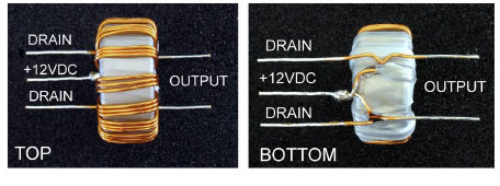
Actual core used in the final breadboard circuit and prototype
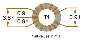
Measured magnetic properties of the inductor