
SCHEMATIC DIAGRAM
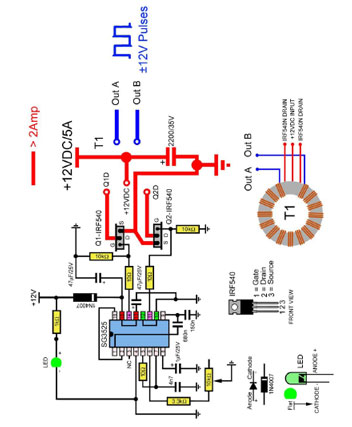
Above is a diagram of the Schematic. There is not a lot to the unit, as most of the hardwork is done by the SG3525AN, hence the attraction for this IC. Pay attention to the high current sections.
PARTS LAYOUT
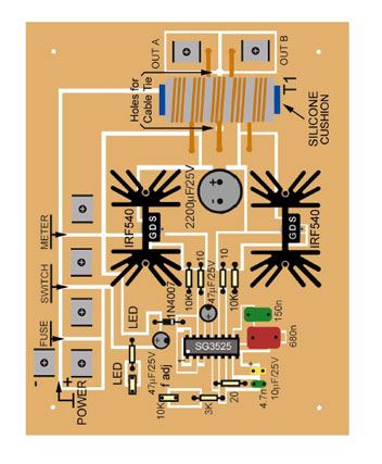
Above is a diagram of the PCB layout. I do not like crowded PCB’s and if size is a concern better use Surface Mount components than thru hole.
HARDWARE LAYOUT
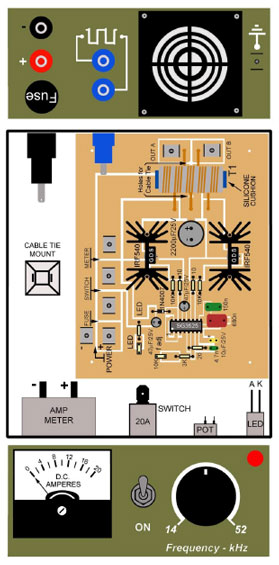
What was used in the unit is obvious. The Banana sockets and associated plugs make setting up very easy.
FACE PLATES
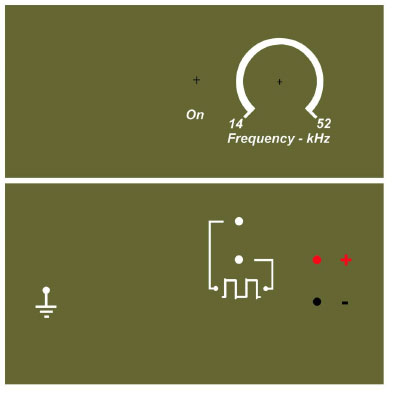
I always like to give my creations a nice panel. Above are the panel templates for the front and rear. These are printed on A4 size shipping labels (the adhesive kind) and then covered with the clear adhesive film – the type used to cover school books. After trimming they are aligned with the holes in the metal work and then carefully placed on the metal work and any excess removed with a craft knife.
DRILLING TEMPLATE
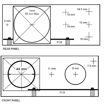
Above is the art work for the drilling template. Again I print this on A4 size shipping labels, trim and then carefully place them on the metal work. To get a good final product it is important to make very careful measurements. You need only two tools for this – observant eyes and a ruler.
SETTING UP THE FLYBACK DRIVER
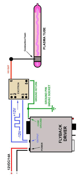
How the Excitron transformer was setup for testing.