
Elapse Timer Project
This chapter shows you how to build an elapse timer using the F88 Experimenter’s Board. We will use 3 I/O pins of F88 Experimenter’s Board to control timer function.
Schematics
A 9V battery powers the whole circuit. It is connected to 9V & Gnd pins of F88 Board as before. 5V is taken out from F88 Board (on-board 5V regulator) for powering external components.
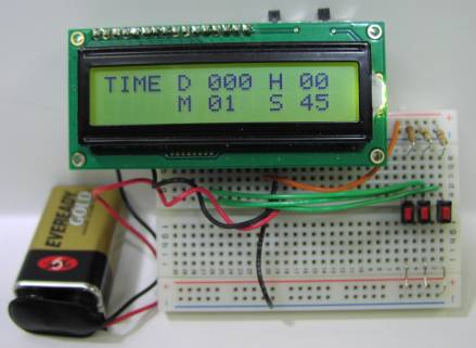
Switch S1 (Momentary, SPST, Push Button) connected to RB4 pin acts as a reset. Pressing this switch will reset the timer to 0. Timer will be in reset till this switch is pressed.
Switch S3 (Latching, SPST, Push Button/Slide/Toggle) connected to RB6 pin acts as enable/trigger. With S3 in its on state, timer will start running. Bringing S3 in its off state will stop the timer. Making it on again, resumes the timer where it left off. A 5V TTL digital signal can replace S3 to control the timer.
Switch S2 (Latching, SPST, Push Button/Slide/Toggle) connected to RB5 pin acts as level selection. It essentially sets which state of S3 runs the timer. If S2 is in its on state, then S3’s on state will run the timer. If S2 is in its off state, then S3’s off state will run the timer. S2 & S3 must be in same state for timer to run, a dissimilar state of S2 & S3 will halt the timer. This functionality helps when a digital signal is used in place of S3. It allows which state of signal (high or low) enables the timer.
R1, R2 & R3 are pull up resistors for switches S1, S2 & S3.