
Introduction
The 16F88 PIC Experimenter's Board is a complete prototyping platform for the 16F88 18-pin PIC microcontroller. This article is one the use of the 16F88 PIC Experimenter's Board. It assumes you already know how to write PICBasic programs, compile the program to a hex file, and upload the hex file (firmware) into the 16F88 PIC Microcontroller. For beginner's needing tutorials on writing PICBasic Programs, compiling and uploading firmware, go here.
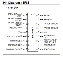 Main 16F88 Features:
Internal Oscillator -plus 3 Xtal Modes up to 20 MHz.
10 Bit, 7 Channel Analog-to-Digital Converter
2 Comparators
Asynchronous Receiver Transmitter
7168 Bytes memory
368 SRAM
256 EEPROM - Data Retention > 40 Years
100,000 erase/write cycles
Operating voltages 2.0V to 5.5V
16F88 PIC Experimenter's board
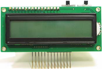
The 16F88 PIC Experimenter's board is designed to be plugged into a solderless bread board connection for quick and easy access to Port A (RA5, RA6, RA7) and Port B (RB0, RB1, RB2, RB4, RB5, RB6, RB7) I/O lines. It includes an integrated 16x2 LCD display with backlight.
PINS or I/O Lines
When discussing connections to the 16F88 I use two terms interchangeably, pins or I/O lines (Input/Output lines). I imagine one could argue the nomenclature, technically pins are on the microcontroller and the I/O lines are the connections to the pins. Beyond this, Input/Output means we can configure the I/O line to be either and input or output line. While the I/O line can not be both input and output simultaneously, the program can switch the lines state from input to output and vice versa. This switching can happen so fast that it may give the impression that it is functioning as both.
Use
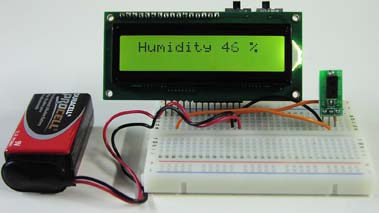
The board can be powered by either a 9V battery or a AC/DC transformer. The power switch in the upper right turns the board on and off. The LCD backlight switch is next to the power switch, located on the right hand side above the LCD.
The prototyping area is as large as the solderless breadboard you plug the 16F88 experimenter's board into. For those who have not dabbled in electronics we will describe the usage of the solderless bread board and wire a simple LED project. See figure 1.
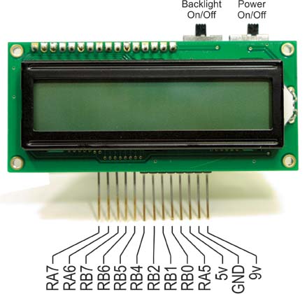
Figure 1
The design and function to solderless breadboards is shown in Figure 2.
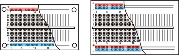
You can breadboard (assemble and connect) electronic components and electronic circuits into the prototyping area without soldering. The prototyping area is reusable; you can change, modify or remove circuit components at any time. This makes it easy to correct any wiring errors. A cutaway of two common solderless breadboards are shown above.
The square holes shown in the area are sockets. When a wire or pin is inserted into a hole, it makes electrical contact with the underlying metal strip. The holes are spaced so that integrated circuits and many other components can be plugged right in.
The internal electrical connection structure of the solderless breadboard is shown in the cutaway.
Simple Experiment:
We shall wire a simple experiment to illustrate the usage of the experimenter's board for prototyping. Before we do so Let's look at a schematic of the circuit on the experimenter's board.
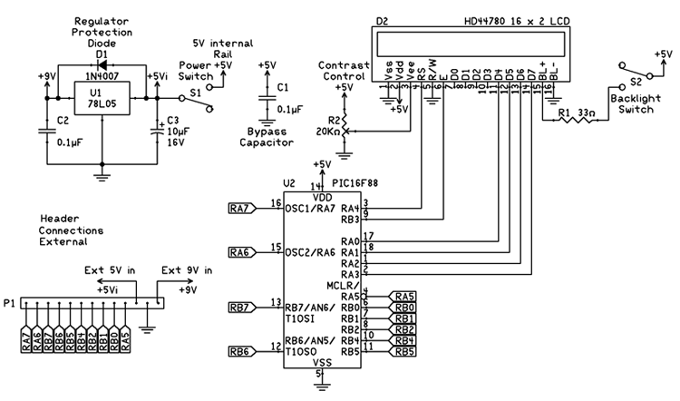
This schematic is comprehensive but not complete. In the full schematic there are options for external crystals on pins 15 and 16, as well as 12 and 13. We are not using crystals in our circuit(s) just yet. Instead we are using the internal oscillator of the 16F88.
We can simplify our schematic even further. It's not necessary to continually show the PIC 16F88, power supply and LCD module. Instead I will only show the header pinout to the experimenter's board along with the rest of the circuit. The schematic below is to blink an LED. The following is a small PBP program to blink an LED on PIN RB1.
PIC 16F88 Configuration Register
The 16F88 has two 14-bit configuration registers at memory locations 2007H and 2008H. The bits in the PIC's configuration register enable or disable features in the microcontroller. Features such as Code Protection, Watchdog timer, Oscillator, etc.
Using PBP compiler and MicroCode Studio IDE allows you to set the configuration switches inside the program. We only need to set a few bit registers and leave the rest at their default status. Add the following three lines to the top of your program to set the configuration switches.
__config _CONFIG1,_INTRC_IO & _WDT_OFF & _PWRTE_ON & _MCLR_OFF & _LVP_OFF & _CP_OFF
#ENDCONFIG
These settings are applicatable for most of our programming needs at this moment. For more information on this Configuration Setup go here.
'BLINK PBP Program 1.1
#CONFIG
__config _CONFIG1,_INTRC_IO & _WDT_OFF & _PWRTE_ON & _MCLR_OFF & _LVP_OFF & _CP_OFF
#ENDCONFIG
osccon = %01110100 'Set-up internal oscillator at 8 MHz
start: 'Start of routine
High PortB.1 'Turn on LED
Pause 500 'Wait 1/2 second
Low PortB.1 'Turn off LED
Pause 500 'Wait 1/2 second
Goto start 'Goto Start and repeat
Download PBP 1.1 Source
Download PBP 1.1 Hex File
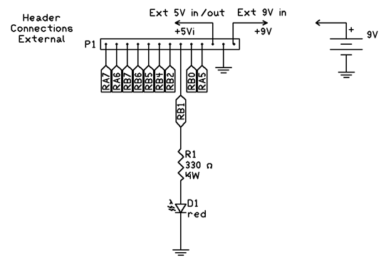
Aside from a programmed 16F88 we only need a 9V battery and two other components; a 330-ohm ¼ watt resistor and a sub-miniature LED. All the other components needed to make the 16F88 work are already hard wired on the PIC Experimenters Board.
The LED has two terminals, one longer than the other. On the schematic it is shown as a diode. The longer terminal on the LED is positive, shown in the legend of figure below.
To wire this circuit, Plug the 16F88 project board into the solderless breadboard. Connect a 9 volt battery to the 9V terminal and ground termin repsectively. Connect a wire from the ground of the 16F88 project board to the ground strip of the solderless breadboard. Shown as the green wire in the drawing. Next connect one lead of the ¼ watt resistor into one of the RB1 sockets. Connect the other lead of the ¼ watt resistor into a socket in Bank 2.
Take the positive lead of the LED and plug it into a socket in the same column as the one containing the resistor lead. Connect the opposite lead of the LED and plug it into one of the ground sockets at the bottom, see figure below.
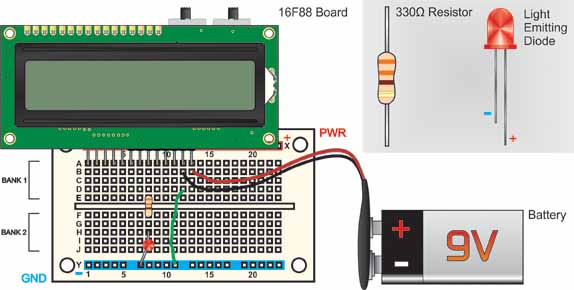
Plug the programmed 16F88 microcontroller into the 18 pin socket on the PIC Experimenters Board and turn on the power. The LED should begin blinking on and off. This on-off cycle (blinking) continually repeats.