When P-type and N-type silicon are placed in contact with one another it forms a PN junction. At this junction an interesting phenomenon occurs, one that is the foundation of solid-state electronics.
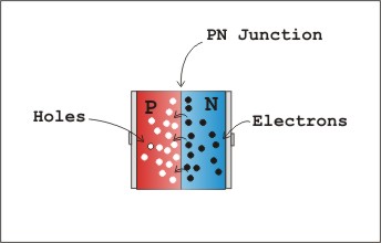
A basic PN junction creates a diode that allows electricity to flow in one direction but not the other. We can see in the diagram of a diode that the N type material has free electrons shown as black dots and the P type material has holes shown as white dots.
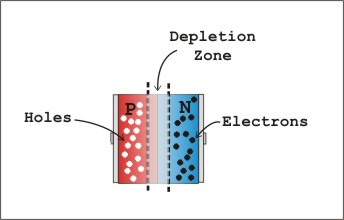
Near the PN junction the electrons diffuse into the vacant holes in the P material causing a depletion zone. This depletion zone acts like an insulator preventing other free electrons in the N-type silicon and holes in the P-type silicon from combining.
In addition this leaves a small electrical imbalance inside the crystal. Since the N region is missing some electrons it has obtained a positive charge. And the extra electrons that filled the holes in the P region, have given it a negative charge. Unfortunately one cannot generate power from this electrical imbalance. However the stage is set to see how the PN junction functions as a diode.
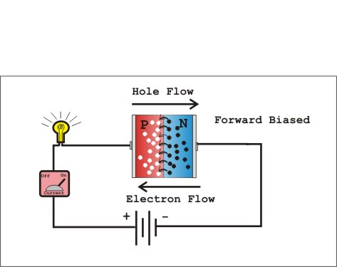
In the next diagram we have connected an external power source; a battery with a light and current meter that indicate current flow. The negative terminal of the battery is connected to the N-type silicon. Like charges repel, so the free electrons are pushed toward the PN junction. Similarly the hole are repelled by the positive terminal of the battery toward the PN junction. If the voltage pushing the electrons and holes has sufficient strength to overcome the depletion zone (approximately 0.7 V for typical silicon diode) the electrons and holes combine at the junction and current passes through the diode. When a diode is arranged this way with a power supply it is said to be forward-biased.
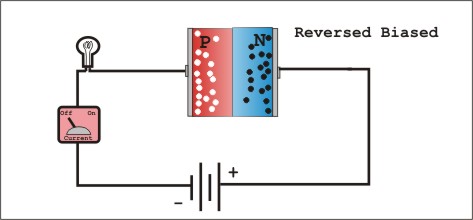
In the last diagram the battery is connect to the diode so that the negative terminal of the battery connects to the P-type silicon and the positive terminal of the battery connects to the N-type silicon. The negative terminal attracts the positive holes in the P-type silicon and the positive terminal of the battery attracts the free electrons in the N-type silicon. All the charge carriers are pulled away from the PN junction which essentially creates a larger depletion region and no current flows. When a diode is arranged this way with a power supply it is said to be reverse-biased.